
F1 Smart Module
Datasheet — March 2024 V1.1
Introduction
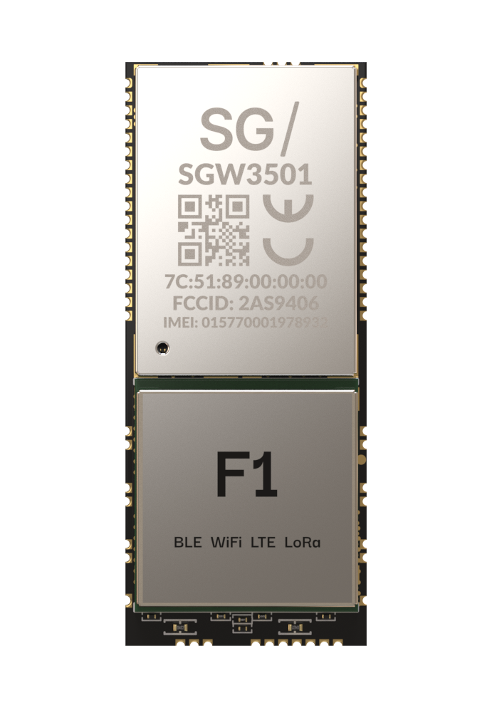
The F1 Smart Module is a compact OEM module equipped with BLE, Wi-Fi, LoRa(WAN), and LTE CAT-M1/NB1/NB2 to support various connectivity needs. Running on a MicroPython-programmable microcontroller with a no-barrier entry into the SG Wireless Ctrl. Cloud Platform, the module enables truly limitless IoT application development with multi-network creation flexibility and rapid scaling capacity.
Key Features
Multi-connectivity:
WiFi 802.11b/g/n (2.4 GHz)
Bluetooth BLE 5.0
Cellular LTE-CAT M1/NB1/NB2
LoRa(WAN) 868 MHz (EU) and 915 MHz (US)
Powerful Espressif ESP32-S3 CPU
MicroPython programmable with 27 IOs on module pads
SMT-friendly semi-hole pins at module edges
Operating temperature: −40 °C to 85 °C
Compact size: 42.67 mm × 17.73 mm × 3.50 mm
Order Information
Part Number |
Description |
|---|---|
SGW3501 |
F1 Smart Module: BLE, WiFi, LoRa, LTE |
SGW3401 |
F1/C Cellular Module: BLE, WiFi and LTE |
SGW3201 |
F1/L LoRa Module: BLE, WiFi and LoRa |
General Features
Feature Specifications
Component |
Specifications |
|---|---|
CPU |
Xtensa® dual-core 32-bit LX7 microprocessor, up to 240 MHz
On-chip 384 KB ROM and 512 KB SRAM, on-board 8 MB PSRAM and 16 MB Flash
Deep Sleep Mode: 10 µA
|
WiFi/BLE |
Espressif ESP32-S3 on-chip RF frontend
WiFi: IEEE 802.11b/g/n (2.4 GHz band); Data Rate: 1 M up to 54 Mbps (MCS7); Max Tx Power: 20 dBm
BLE: Bluetooth LE 5.0, Bluetooth mesh; Data Rate: 125 kbps to 2 Mbps; Max Tx Power: 20 dBm
|
LTE |
Sequans Monarch2 GM02S for CAT-M1, CAT-NB1 and CAT-NB2 support
LTE CAT-M1/NB1/NB2 transmit power up to +23 dBm
PTCRB and GCF 1.3 3GPP release 13 compliant; Operator Approval: Verizon, AT&T, T-Mobile, Vodafone, Orange
|
LoRa(WAN) |
Semtech SX1262 RF transceiver, 868/915 MHz LPWAN Module
TX Power: Up to +22 dBm; Sensitivity: −127 dBm
LoRaWAN stack – Class A and Class C Device
|
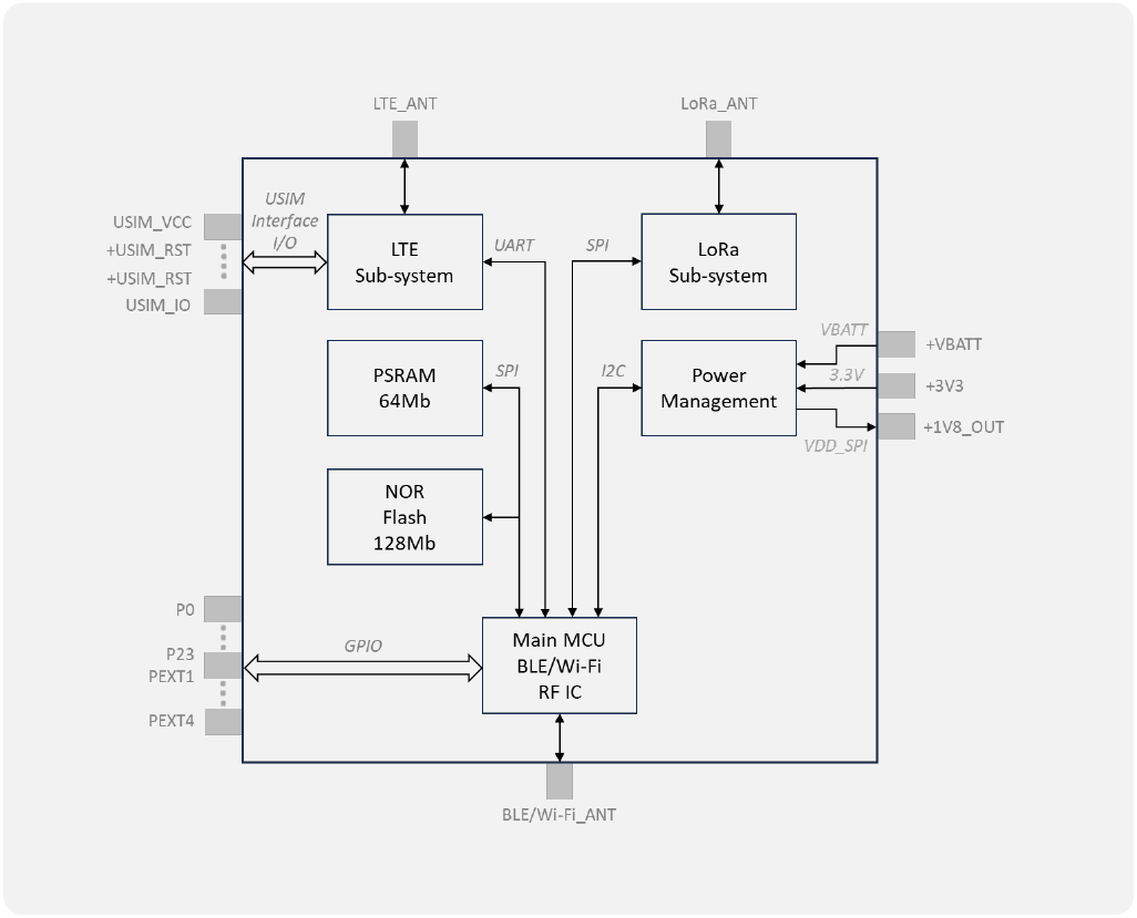
Figure 1: F1 Smart Module Block Diagram
Pinout & Pin Definitions
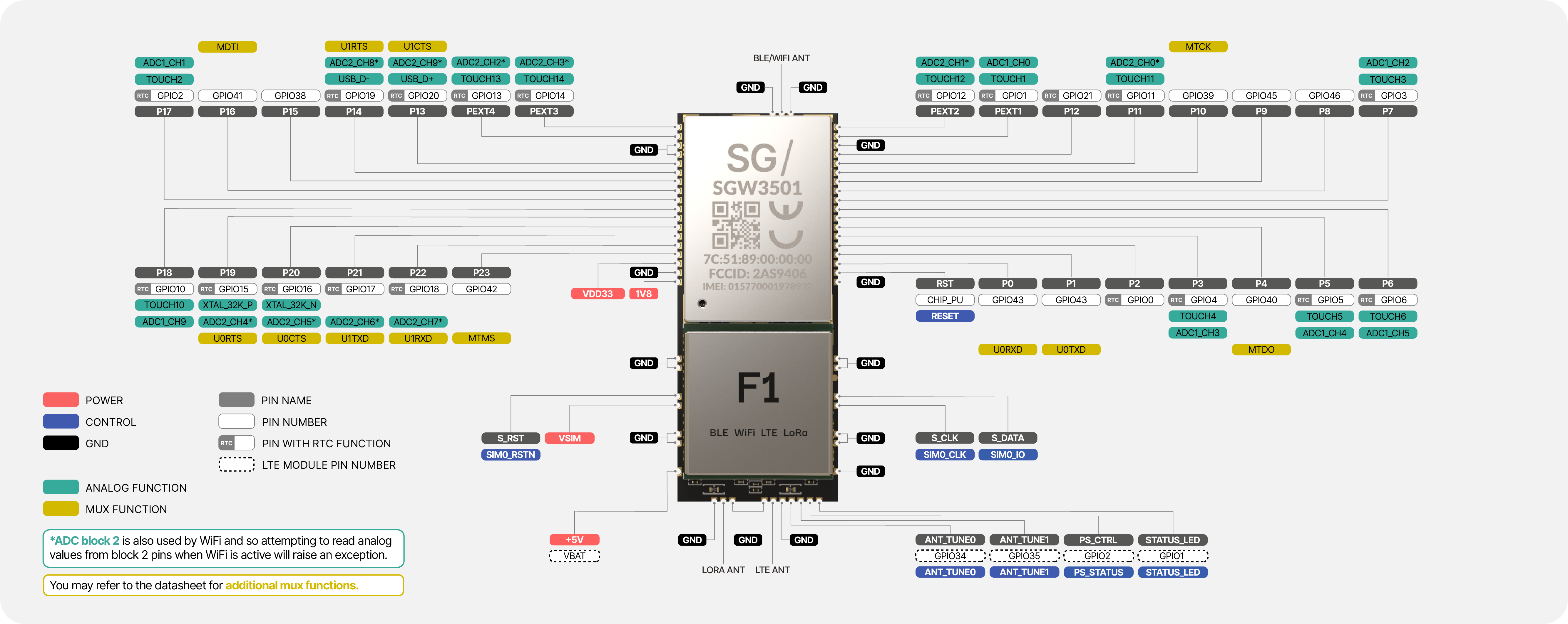
Figure 1: F1 Smart Module Pinout Diagram
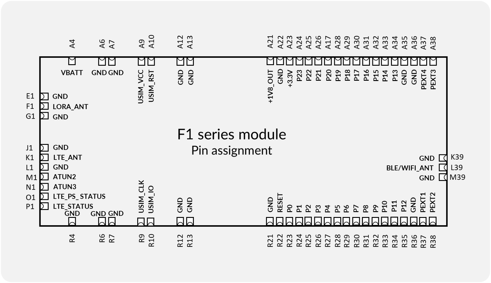
Figure 2: F1 Smart Module Pin-out (Top View)
Kindly refer to the Mechanical Specifications section for more details on the physical dimensions.
Pin Definitions
Pin Number |
Pin Name |
MCU Pin |
LTE Module Pin |
Type |
Description |
|---|---|---|---|---|---|
R4 |
GND |
Power |
Ground signal |
||
R6 |
GND |
Power |
Ground signal |
||
R7 |
GND |
Power |
Ground signal |
||
R9 |
USIM_CLK |
SIM0_CLK |
Analog I/O |
USIM interface I/O to GM02S |
|
R10 |
USIM_IO |
SIM0_IO |
Digital I/O |
USIM interface I/O to GM02S |
|
R12 |
GND |
Power |
Ground signal |
||
R21 |
GND |
Power |
Ground signal |
||
R22 |
RESET |
CHIP_PU |
Analog I/O |
Reset pin to ESP32-S3 for module reset |
|
R23 |
P0 |
U0RXD |
Analog I/O |
UART0 RXD to ESP32-S3 |
|
R24 |
P1 |
U0TXD |
Analog I/O |
UART0 TXD to ESP32-S3 |
|
R25 |
P2 |
GPIO0 |
Analog I/O or Digital I/O |
Analog I/O or Digital I/O to ESP32-S3 |
|
R26 |
P3 |
GPIO4 |
Analog I/O or Digital I/O |
Analog I/O or Digital I/O to ESP32-S3 |
|
R27 |
P4 |
MTDO |
Digital I/O |
Digital I/O to ESP32-S3 |
|
R28 |
P5 |
GPIO5 |
Analog I/O or Digital I/O |
Analog I/O or Digital I/O to ESP32-S3 |
|
*R29 |
P6 |
GPIO6 |
Reserved – Leave floating, do not connect |
||
R30 |
P7 |
GPIO3 |
Analog I/O or Digital I/O |
Analog I/O or Digital I/O to ESP32-S3 |
|
R31 |
P8 |
GPIO46 |
Digital I/O |
Digital I/O to ESP32-S3 |
|
R32 |
P9 |
GPIO45 |
Digital I/O |
Digital I/O to ESP32-S3 |
|
R33 |
P10 |
MTCK |
Digital I/O |
Digital I/O to ESP32-S3 |
|
R34 |
P11 |
GPIO11 |
Analog I/O or Digital I/O |
Analog I/O or Digital I/O to ESP32-S3 |
|
R35 |
P12 |
GPIO21 |
Analog I/O or Digital I/O |
Analog I/O or Digital I/O to ESP32-S3 |
|
R36 |
GND |
Power |
Ground signal |
||
R37 |
PEXT1 |
GPIO1 |
Analog I/O or Digital I/O |
Analog I/O or Digital I/O to ESP32-S3 |
|
R38 |
PEXT2 |
GPIO12 |
Analog I/O or Digital I/O |
Analog I/O or Digital I/O to ESP32-S3 |
|
M39 |
GND |
Power |
Ground signal |
||
L39 |
BLE/WIFI_ANT |
RF I/O |
RF interface to ESP32-S3 for BLE and/or Wi-Fi interface |
||
K39 |
GND |
Power |
Ground signal |
||
A38 |
PEXT3 |
GPIO14 |
Analog I/O or Digital I/O |
Analog I/O or Digital I/O to ESP32-S3 |
|
A37 |
PEXT4 |
GPIO13 |
Analog I/O or Digital I/O |
Analog I/O or Digital I/O to ESP32-S3 |
|
A36 |
GND |
Power |
Ground signal |
||
A35 |
GND |
Power |
Ground signal |
||
A34 |
P13 |
GPIO20 |
Analog I/O or Digital I/O |
Analog I/O or Digital I/O to ESP32-S3 / USB OTG D+ |
|
A33 |
P14 |
GPIO19 |
Analog I/O or Digital I/O |
Analog I/O or Digital I/O to ESP32-S3 / USB OTG D− |
|
A32 |
P15 |
GPIO38 |
Digital I/O |
Digital I/O to ESP32-S3 |
|
A31 |
P16 |
GPIO41 |
Digital I/O |
Digital I/O to ESP32-S3 |
|
A30 |
P17 |
GPIO2 |
Analog I/O or Digital I/O |
Analog I/O or Digital I/O to ESP32-S3 |
|
A29 |
P18 |
GPIO10 |
Analog I/O or Digital I/O |
Analog I/O or Digital I/O to ESP32-S3 |
|
A28 |
P19 |
GPIO15 |
Analog I/O or Digital I/O |
Analog I/O or Digital I/O to ESP32-S3 |
|
A27 |
P20 |
GPIO16 |
Analog I/O or Digital I/O |
Analog I/O or Digital I/O to ESP32-S3 |
|
A26 |
P21 |
GPIO17 |
Analog I/O or Digital I/O |
Analog I/O or Digital I/O to ESP32-S3 |
|
A25 |
P22 |
GPIO18 |
Analog I/O or Digital I/O |
Analog I/O or Digital I/O to ESP32-S3 |
|
A24 |
P23 |
GPIO42 |
Digital I/O |
Digital I/O to ESP32-S3 |
|
A23 |
+3.3V |
VDD3P3_CPU VDD3P3_RTC VDD3P3 VDDA |
Power |
Voltage supply to ESP32-S3 and module main circuit |
|
A22 |
GND |
Power |
Ground signal |
||
A21 |
+1.8V_OUT |
VDD_SPI |
Power |
Voltage supply VDD_SPI to ESP32-S3 for SPI flash and PSRAM |
|
A13 |
GND |
Power |
Ground signal |
||
A12 |
GND |
Power |
Ground signal |
||
A10 |
USIM_RST |
SIM0_RSTN |
Digital I/O |
USIM interface I/O to GM02S |
|
A9 |
USIM_VCC |
SIM0_VCC |
Power |
USIM voltage supply to GM02S |
|
A7 |
GND |
Power |
Ground signal |
||
A6 |
GND |
Power |
Ground signal |
||
A4 |
+VBATT |
VBAT |
Power |
Voltage supply to GM02S |
|
E1 |
GND |
Power |
Ground signal |
||
F1 |
LORA_ANT |
RF I/O |
RF interface to SX1262 for LoRa interface |
||
G1 |
GND |
Power |
Ground signal |
||
J1 |
GND |
Power |
Ground signal |
||
K1 |
LTE_ANT |
LTE_ANT |
RF I/O |
RF interface to GM02S for LTE CAT-M1/CAT-NB1/CAT-NB2 interface |
|
L1 |
GND |
Power |
Ground signal |
Electrical Specifications
Rating & Operating Conditions
Table 1: Absolute Rating and Operating Conditions Specifications
Symbol |
Parameter |
Min |
Typ |
Max |
Unit |
|---|---|---|---|---|---|
Absolute Rating |
|||||
+VBATT |
Supply voltage to Sequans GM02S LTE module |
5.0 |
5.8 |
V |
|
+3V3 |
Supply voltage to Espressif ESP32-S3 and module main circuit |
3.0 |
3.3 |
3.6 |
V |
+1V8_OUT* |
SPI supply voltage (output) of SPI flash and PSRAM for decoupling capacitor connection |
1.8 |
2.3 |
V |
|
T(OPR) |
Operating temperature |
−40 |
85 |
°C |
|
Operating Conditions |
|||||
+VBATT |
Supply voltage to Sequans GM02S LTE module |
2.5 |
5.0 |
5.5 |
V |
+3V3 |
Supply voltage to Espressif ESP32-S3 and module main circuit |
3.2 |
3.3 |
3.4 |
V |
+1V8_OUT* |
SPI supply voltage (output) of SPI flash and PSRAM for decoupling capacitor connection |
1.7 |
1.8 |
1.9 |
V |
CPU IO (3.3 V power domain, VDD = 3.3 V) |
|||||
VIH |
Input high voltage for GPIOs |
0.75 × VDD |
VDD + 0.3 |
V |
|
VIL |
Input low voltage for GPIOs |
−0.3 |
0.25 × VDD |
V |
|
VOH |
Output high voltage for GPIOs |
0.8 × VDD |
V |
||
VOL |
Output low voltage for GPIOs |
0.1 × VDD |
V |
||
Radio IO (1.8 V power domain) |
|||||
VIH |
Input high voltage for GPIOs |
1.26 |
1.8 |
V |
|
VIL |
Input low voltage for GPIOs |
0 |
0.54 |
V |
|
VOH |
Output high voltage for GPIOs |
1.44 |
1.8 |
V |
|
VOL |
Output low voltage for GPIOs |
0 |
0.36 |
V |
* The +1V8_OUT pin is to connect an external capacitor to the module internal SPI flash and PSRAM for a more robust VDD_SPI supply. This pin should not be connected to any external circuits that may draw more than 20 mA. Voltage of this pin will vary in module light sleep mode and approach zero in module deep sleep mode.
WiFi
Standard: 802.11b/g/n (2.4 GHz ONLY) – 1T1R
Table 2: WiFi Specifications
Parameter |
Description |
Min |
Typ |
Max |
Unit |
|---|---|---|---|---|---|
General |
|||||
Freq. (EU) |
Operating frequency (EU) |
2.402 |
2.482 |
GHz |
|
Ch. (EU) |
Channel (EU) |
1 |
13 |
||
Freq. (US) |
Operating frequency (US) |
2.402 |
2.472 |
GHz |
|
Ch. (US) |
Channel (US) |
1 |
11 |
||
Power max. (EU/US) |
Maximum power (EU/US) |
20 |
dBm |
||
Tx |
|||||
Tx Power @B – 1 Mbps |
Tx power at B mode with data rate 1 Mbps |
18 |
20 |
dBm |
|
EVM (Peak) @B – 1 Mbps |
EVM (Peak) at B mode with data rate 1 Mbps |
8 |
% |
||
Freq. Err. @B – 1 Mbps |
Frequency error at B mode with data rate 1 Mbps |
−40 |
0 |
40 |
kHz |
Tx Power @G – 54 Mbps |
Tx power at G mode with data rate 54 Mbps |
16 |
20 |
dBm |
|
EVM (RMS) @G – 54 Mbps |
EVM (RMS) at G mode with data rate 54 Mbps |
−25 |
dB |
||
Freq. Err. @G – 54 Mbps |
Frequency error at G mode with data rate 54 Mbps |
−40 |
0 |
40 |
kHz |
Tx Power @N20 – MCS7 |
Tx power at N mode with data rate MCS7 and 20 MHz bandwidth |
15 |
20 |
dBm |
|
EVM (RMS) @N20 – MCS7 |
EVM rms at N mode with data rate MCS7 and 20 MHz bandwidth |
−27 |
dB |
||
Freq. Err. @N20 – MCS7 |
Frequency error at N mode with data rate MCS7 and 20 MHz bandwidth |
−40 |
0 |
40 |
kHz |
Rx |
|||||
Rx Sens. @B – 1 Mbps |
Rx sensitivity at B mode with data rate 1 Mbps |
−92.0 |
−82.0 |
dBm |
|
Rx Sens. @G – 54 Mbps |
Rx sensitivity at G mode with data rate 54 Mbps |
−76.5 |
−66.0 |
dBm |
|
Rx Sens. @N20 – MCS7 |
Rx sensitivity at N mode with data rate MCS7 and 20 MHz bandwidth |
−71.4 |
−64.0 |
dBm |
Bluetooth
Standard: BLE 5.0 – 1T1R
Table 3: Bluetooth Specifications
Parameter |
Description |
Min |
Typ |
Max |
Unit |
|---|---|---|---|---|---|
General |
|||||
Freq. |
Operating frequency |
2.4000 |
2.4835 |
GHz |
|
Ch. |
Channel |
0 |
39 |
||
Power max. |
Maximum power |
20 |
dBm |
||
Tx |
|||||
Tx Power @Ch.37 – 1 Mbps |
Tx power at channel 37 (freq. = 2402 MHz) with data rate 1 Mbps |
17 |
20 |
dBm |
|
Freq. Err. @Ch.37 – 1 Mbps |
Frequency error at channel 37 (freq. = 2402 MHz) with data rate 1 Mbps |
−50 |
0 |
50 |
kHz |
Tx Power @Ch.38 – 1 Mbps |
Tx power at channel 38 (freq. = 2426 MHz) with data rate 1 Mbps |
17 |
20 |
dBm |
|
Freq. Err. @Ch.38 – 1 Mbps |
Frequency error at channel 38 (freq. = 2426 MHz) with data rate 1 Mbps |
−50 |
0 |
50 |
kHz |
Tx Power @Ch.39 – 1 Mbps |
Tx power at channel 39 (freq. = 2480 MHz) with data rate 1 Mbps |
17 |
20 |
dBm |
|
Freq. Err. @Ch.39 – 1 Mbps |
Frequency error at channel 39 (freq. = 2480 MHz) with data rate 1 Mbps |
−50 |
0 |
50 |
kHz |
Rx |
|||||
Rx Sens. @Ch.38 – 2 Mbps |
Rx sensitivity at channel 38 (freq. = 2426 MHz) with data rate 2 Mbps |
−93.5 |
dBm |
||
Rx Sens. @Ch.38 – 1 Mbps |
Rx sensitivity at channel 38 (freq. = 2426 MHz) with data rate 1 Mbps |
−97.5 |
−70.0 |
dBm |
|
Rx Sens. @Ch.38 – 500 kbps |
Rx sensitivity at channel 38 (freq. = 2426 MHz) with data rate 500 kbps |
−100.0 |
dBm |
LTE
Standard: CAT-M1, CAT-NB1, CAT-NB2
Table 4: LTE Frequency Bands (in MHz)
Band |
Duplex |
Uplink Freq. (MHz) |
UL BW (MHz) |
Downlink Freq. (MHz) |
DL BW (MHz) |
LTE-M |
NB-IoT |
|---|---|---|---|---|---|---|---|
1 |
FDD |
1920 – 1980 |
60 |
2110 – 2170 |
60 |
Yes |
Yes |
2 |
FDD |
1850 – 1910 |
60 |
1930 – 1990 |
60 |
Yes |
Yes |
3 |
FDD |
1710 – 1785 |
75 |
1805 – 1880 |
75 |
Yes |
Yes |
4 |
FDD |
1710 – 1755 |
45 |
2110 – 2155 |
45 |
Yes |
Yes |
5 |
FDD |
824 – 849 |
25 |
869 – 894 |
25 |
Yes |
Yes |
8 |
FDD |
880 – 915 |
35 |
925 – 960 |
35 |
Yes |
Yes |
12 |
FDD |
699 – 716 |
17 |
729 – 746 |
17 |
Yes |
Yes |
13 |
FDD |
777 – 787 |
10 |
746 – 756 |
10 |
Yes |
Yes |
14 |
FDD |
788 – 798 |
10 |
758 – 768 |
10 |
Yes |
Yes |
17 |
FDD |
704 – 716 |
12 |
734 – 746 |
12 |
No |
Yes |
18 |
FDD |
815 – 830 |
15 |
860 – 875 |
15 |
Yes |
Yes |
19 |
FDD |
830 – 845 |
15 |
875 – 890 |
15 |
Yes |
Yes |
20 |
FDD |
832 – 862 |
30 |
791 – 821 |
30 |
Yes |
Yes |
25 |
FDD |
1850 – 1915 |
65 |
1930 – 1995 |
65 |
Yes |
Yes |
26 |
FDD |
814 – 849 |
35 |
859 – 894 |
35 |
Yes |
Yes |
28 |
FDD |
703 – 748 |
45 |
758 – 803 |
45 |
Yes |
Yes |
66 |
FDD |
1710 – 1780 |
70 |
2110 – 2200 |
90 |
Yes |
Yes |
85 |
FDD |
698 – 716 |
18 |
728 – 746 |
18 |
Yes |
Yes |
Table 5: LTE Specifications
Parameter |
Description |
Min |
Typ |
Max |
Unit |
|---|---|---|---|---|---|
General |
|||||
Power max. |
Maximum power |
23 |
dBm |
||
Tx |
|||||
Tx Power @Band 8 (900 MHz GSM) |
Tx power at Band 8 (900 MHz GSM) |
22 |
23 |
dBm |
|
Tx Power @Band 2 (1900 MHz PCS) |
Tx power at Band 2 (1900 MHz PCS) |
22 |
23 |
dBm |
|
Rx |
|||||
Rx sens. @Band 8 (900 MHz GSM) |
Rx sensitivity at Band 8 (900 MHz GSM) |
−103 |
−100 |
dBm |
|
Rx sens. @Band 2 (1900 MHz PCS) |
Rx sensitivity at Band 2 (1900 MHz PCS) |
−103 |
−100 |
dBm |
LoRa(WAN)
Table 6: LoRa(WAN) Specifications
Parameter |
Description |
Min |
Typ |
Max |
Unit |
|---|---|---|---|---|---|
General |
|||||
Freq. (EU) |
Frequency band (EU) |
863 |
870 |
MHz |
|
Freq. (US) |
Frequency band (US) |
902 |
928 |
MHz |
|
Power max. (EU) |
Maximum power (EU) |
15 |
dBm |
||
Power max. (US) |
Maximum power (US) |
22 |
dBm |
||
Tx |
|||||
Tx power @866.4 MHz [EU868] |
Tx power (Tx tone) at 866.4 MHz |
14 |
15 |
dBm |
|
Tx power @918.2 MHz [US915] |
Tx power (Tx tone) at 918.2 MHz |
21 |
22 |
dBm |
|
Rx |
|||||
Rx Sens. @866.4 MHz, BW=500 kHz, SF=12 |
Rx sensitivity at 866.4 MHz, 500 kHz bandwidth and SF=12 |
−127 |
dBm |
Module Interface
Power Management
Table 7: Power Consumption by Mode of Operation
Mode of Operation |
Min |
Typ |
Max |
Unit |
|---|---|---|---|---|
Idle (no radio but MicroPython is running) |
30 |
mA |
||
Light sleep (wake up or restart is required for MicroPython to run) |
800 |
µA |
||
Deep sleep (wake up or restart is required for MicroPython to run) |
10 |
µA |
Memory Allocation
Module OS firmware, OTA and user space sizes:
Module OS firmware: 2,560 KB
OTA1 space: 2,560 KB
OTA2 space: 2,560 KB
User space: 8 MB
Mechanical Specifications
Module Dimensions
All pins have a pin width of 0.7 mm with the exception of pin VBATT (pin #A4) with a 1.0 mm width.
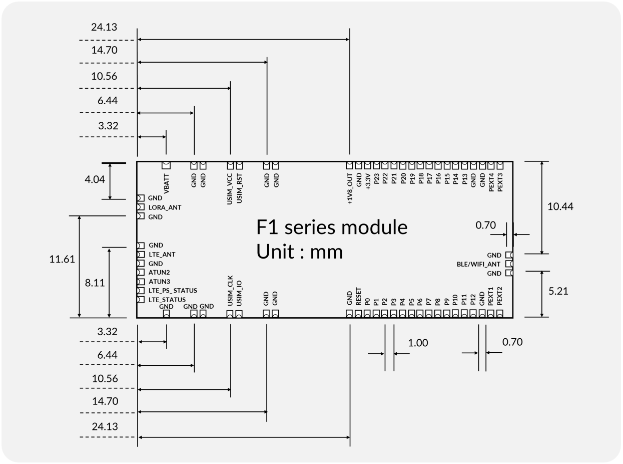
Figure 4: F1 Smart Module Dimensions
Recommended PCB Landing Pattern
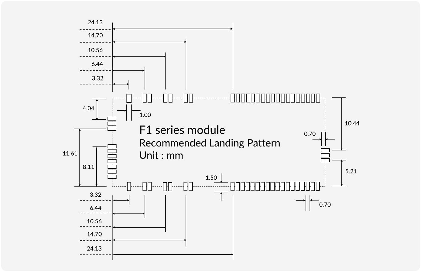
Figure 5: Recommended PCB Landing Pattern (Top View)
Recommended Soldering Profile
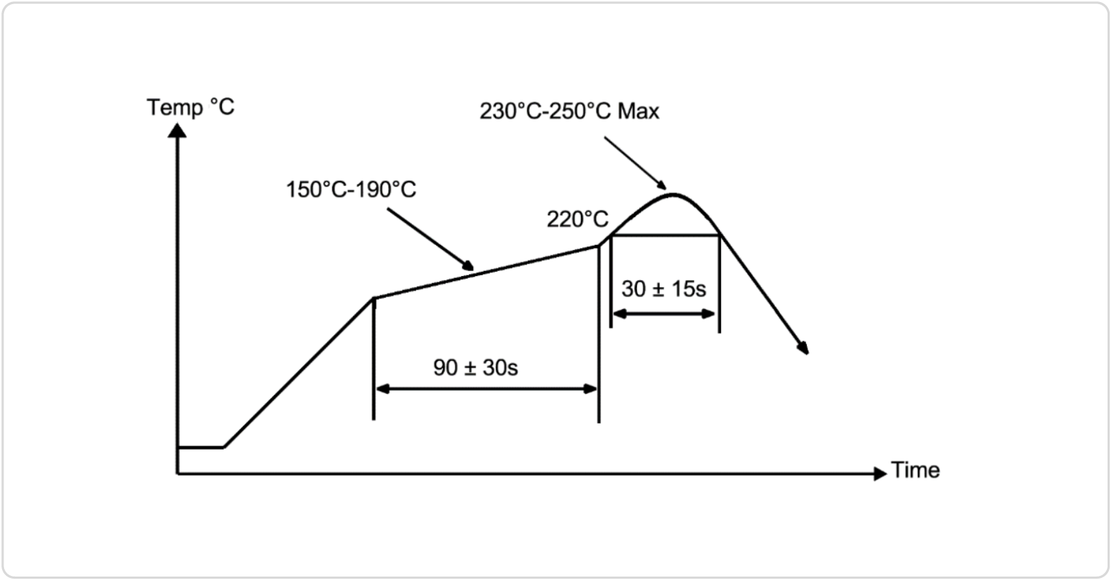
Figure 6: Recommended Soldering Profile
MicroPython
Device Programming via UART
By default, the F1 Smart Module runs an interactive Python REPL (Read-Eval-Print Loop) on UART0 which is connected to P0 (RX) and P1 (TX) running at 115200 baud.
The module can be connected via a development board or any USB UART adapter. Code can be run via the REPL and the SG Wireless Ctrl. Visual Studio Code plug-in can also be used to upload code to the board.
Module-supported Libraries
Table 9: F1 Smart Module Supported Libraries
Library |
Description |
|---|---|
Python Standard Libraries |
array, asyncio, binascii, builtins, cmath, collections, errno, gc, gzip, hashlib, heapq, io, json, math, os, platform, random, re, select, socket, ssl, struct, sys, time, zlib, _thread |
MicroPython-specific Libraries |
Bluetooth, btree, cryptolib, deflate, framebuf, machine, micropython, neopixel, network, uctypes, esp, esp32 |
SGW3501 Module-specific Libraries |
lte: Ready-to-use LTE CAT-M1/NB1/NB2 library
lora: Ready-to-use LoRa RAW and full stack LoRa WAN device Class A, Class C library
ctrl: Ready-to-use Ctrl Cloud Platform client library
|
Note
MicroPython documentation library with API function calls: https://docs.micropython.org/. Libraries may vary by version – please check the latest F1 Module firmware release note for the required library (pre-loaded onto Module).
Product Packaging
Modules are packed in tape-and-reel packaging and shipped out in carton boxes.
Tape – MSL (Moisture Sensitivity Level): 3
Reel – 250 pcs per reel
Note
All units are in millimetres.
Revision History
Version |
Released Date |
Description |
|---|---|---|
1.0 |
Feb 7, 2024 |
Initial document release |
2.0 |
Aug 8, 2024 |
Add Certification information |
Certification
Model |
Certification Type |
Description |
|---|---|---|
F1 |
CE Certificate |
CE certificate of F1 (Type designation: SGW3501) |
F1/C |
CE Certificate |
CE certificate of F1/C (Type designation: SGW3401) |
F1/L |
CE Certificate |
CE certificate of F1/L (Type designation: SGW3201) |
F1 |
FCC Certificates |
FCC certificates of F1 (Type designation: SGW3501) |